

Physical Design Services
Expert Design Services in Synthesis / DFT / PD / STA on designs
with stringent PPA (Power, Performance & Area) requirements
Physical Design Services
MosChip specializes in RTL to GDSII using both Cadence and Synopsys flows. We not only maintain leading EDA infrastructure for physical design, but also employ a team with dedicated subject matter experts with rich experience in the physical design flow and methodologies critical to achieving optimum performance, power, and area (PPA).
Our proven flows and methodologies ensure that the design gets through the range of foundry-specific DRCs, LVS, and ERCs precisely to avoid multiple iterations to avoid delays and stay on schedule.
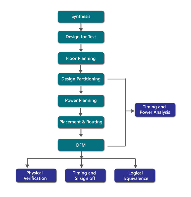
Our key offerings as part of our Physical Design services encompasses the following:
- RTL Synthesis
- Design for Test (Scan, ATPG, MBIST, LBIST)
- Design Partitioning
- Qualifying Libraries and Design Constraints
- Low Power Design
- IO Planning, Floor-Planning, Power Planning
- Place & Route
- Clock-Tree synthesis
- DFM/DFY
- Full-chip timing/SI closure, static timing analysis, and sign-off
- Logical Equivalence Checks
- Physical Verification (LVS, DRC, ERC)
- ECO Iterations for Functional and Timing fixes
We help our customers make the choice of the foundry for tape-out, which is one of the most critical aspects of the process. MosChip closely works with leading foundries including TSMC, GF, etc. Over the last 20+ years, MosChip has been involved in Synthesis, Physical Design, and Timing Closure on quite a few multi-million gate chips with frequencies running up to 1.2GHZ and with low power intent implemented.
MosChip has been involved in tape-outs targeted to 14nm/10nm/7nm process nodes. MosChip team has experience with TSMC, Global, and Samsung Foundries. MosChip has developed synthesis, physical design, and timing flow that has been successfully used on a large number of designs. The team has strong expertise in implementing low-power techniques – Clock Gating, Multi-Vt, Voltage Islands, and Power Gating.
Our Expertise
- Constraints Preparation and Validation
- Logic Synthesis and Physical Synthesis
- Physical Design (IO ring, Floorplanning, PG Planning, Place, Optimization for Timing and Power, Clock Tree Synthesis, Routing, Post Route Optimization)
- Low Power Expertise – Clock Gating, Multi-Vt, Voltage Islands, Power Gating
- EM & IR drop analysis, SI Closure
- Timing Closure and Static Timing Analysis
- Physical Verification (DRC/ERC/LVS)
- Foundries: TSMC, UMC, Global Foundry, IBM, Tower Jazz, and Samsung
- 180nm all the way down to 16nm/14nm/10nm/7nm