

Strategies for FPGA to ASIC Migration for Product Teams
An FPGA is a first choice for product teams; it can take a product from concept to a working system quickly. Product teams can validate the design in hardware, change features, fix bugs, and iterate without committing to silicon.
But at scale, the design eventually reaches to a certain point where the cost of retaining FPGA-based implementation outweighs the value of its flexibility. FPGAs can also become restrictive as product requirements push for lower power, higher performance, or a smaller form factor. At higher volumes, the recurring cost of using an FPGA can become difficult to justify. There may also be a need to integrate more functions into a single device.
This is the point when FPGA-to-ASIC migration becomes worth considering.
FPGA-to-ASIC migration is sometimes treated as a simple RTL conversion, which is not an ideal starting point. An FPGA design that has been proven in hardware provides a strong foundation and reduces technical uncertainty around the product’s functionality. It does not, however, eliminate the ASIC-specific challenges of implementation, IP integration, verification, DFT, and manufacturing. The migration must therefore determine what can be carried forward and what needs to be replaced, redesigned, or revalidated for production silicon.
The main task is to decide what to preserve, what to replace, and what to redesign when migrating.
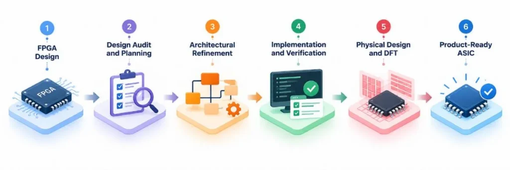
Before starting the migration, establish what is being changed.
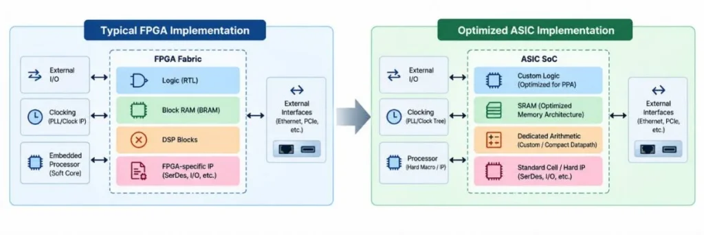
An FPGA implementation can contain portable RTL alongside vendor-specific IP, block RAMs, DSP resources, SerDes, clocking primitives, embedded processors, and dedicated I/O structures. Some of these elements can be replaced with ASIC equivalents. Others may need substantial work.
This audit should go beyond an RTL inventory. Teams should examine why particular resources were used in the first place. An architecture may contain workarounds that made perfect sense on the FPGA but become unnecessary, or even counterproductive, in an ASIC.
The objective is to retain proven product functionality while shedding assumptions that belong to the FPGA platform.
A working FPGA hardware design has already been through simulation, debugging, timing fixes, integration issues, and probably a few architectural compromises along the way.
FPGA architectures are influenced by the resources available on the device. Designers may introduce additional parallelism to meet throughput targets, distribute logic around available resources, or organize memories around fixed block RAM configurations.
An ASIC removes many of these constraints, which creates room to rethink the architecture rather than simply redo the FPGA implementation.
The migration should revisit the datapath, pipeline depth, parallelism, memory organization, interfaces, clock domains, and data movement.
Consider an FPGA design that relies heavily on DSP blocks for arithmetic. That choice may be the case when the FPGA is the target. In an ASIC design, dedicated arithmetic logic can be tailored to the workload, which may change the balance of power, area, and performance. The same applies to memory. Several FPGA memories may make sense because of the resources available on the device, while an ASIC may benefit from consolidating them into a more suitable SRAM architecture.
There is no point in carrying every FPGA decision into the ASIC.
The point is not to discard RTL that already works or redesign the chip simply because the technology has changed. It is to separate the decisions driven by the product requirements from those driven by the FPGA fabric. The first ones are worth protecting. The second ones deserve another look.
PPA are often cited as the primary reason for moving to an ASIC. They should be quantified before implementation gets underway.
The design needs real targets. Performance targets should define operating frequency, latency, throughput, and interface bandwidth. Power targets should reflect real-world workloads and operating states rather than being defined without reference to how the product will be used. Area targets should cover logic, memories, interfaces, and other IP that will occupy the die.
These parameters are closely entangled. We cannot adjust one without impacting the others.
There are no universal PPA targets that work for every silicon. A battery-powered device may place power at the top of the list. A high-throughput networking device may have a very different hierarchy of constraints. The important part is to make those trade-offs explicit.
The actual ASIC migration plan should have a measurable purpose. Lower power, higher performance, smaller silicon area, reduced recurring cost, or a combination of these should be established as design objectives rather than discovered halfway through implementation.
The FPGA prototype and its verification environment are valuable assets during migration.
Existing testbenches, test vectors, assertions, and system-level tests can often be reused as the foundation for ASIC verification.
Formal checks, equivalence verification, CDC analysis, and targeted simulation can help establish that the migrated design still behaves as intended.
The principle is simple: reuse the verification work, but do not assume FPGA validation automatically translates to ASIC sign-off.
ASIC migration also introduces physical implementation and manufacturing considerations that are less visible in an FPGA design.
Floorplanning, timing closure, clocking, power integrity, and routing can influence architectural decisions. DFT requirements such as scan, ATPG, and memory test should also be considered early. Bringing physical design and DFT inputs into the process early can expose architectural constraints while they are still relatively easy to address. Changes discovered late in the ASIC flow can require RTL rework, affect the schedule, and increase the risk of a costly silicon respin.
These areas do not need to drive the migration strategy, but they should be considered early enough to avoid late design changes.
Before committing to the migration, the team should examine:
The engineering case and the commercial case need to converge before the migration begins.
To summarize, FPGA-to-ASIC migration is often described as a technology transition. It is better understood as a transition from a flexible implementation to a purpose-built product.
The migration starts by separating portable RTL from FPGA-specific dependencies. It then revisits the architecture, establishes PPA targets, carries forward useful verification assets, and accounts for physical design and manufacturing requirements early in the process.
The central question is: what should change before the proven FPGA design becomes production-ready silicon?
That question turns migration from a straightforward technology swap into an opportunity to build silicon that is better aligned with the product’s actual requirements.
For product teams, the migration often spans several engineering disciplines, from RTL through verification, physical implementation, IP integration, and silicon bring-up. MosChip helps take proven FPGA design towards production-ready ASICs, covering the turnkey ASIC cycle from RTL design through tape-out and volume production. MosChip’s silicon engineering expertise helps identify FPGA-specific dependencies, refine the architecture, and optimize, migrate the design for the target PPA and process requirements.
Want to explore FPGA product development beyond RTL?
Watch our recent webinar, “Engineering FPGA Products: Moving Beyond the RTL,” to learn how teams bridge hardware, software, processing systems, and validation to build production-ready FPGA platforms.
MosChip supports the migration of proven FPGA designs toward production-ready ASICs, covering design audit, architectural refinement, RTL design, verification, physical design, DFT, and silicon bring-up.
Yes. MosChip can assess the existing FPGA design to identify reusable RTL, FPGA-specific resources, vendor-dependent IP, and areas that require replacement or architectural redesign.
Yes. MosChip can help define and optimize the ASIC architecture against power, performance, and area targets while considering the trade-offs associated with architectural changes.
MosChip can build on existing FPGA verification assets, including testbenches, test vectors, assertions, and system-level tests, while applying ASIC-specific verification such as equivalence checking, formal verification, and CDC analysis.
MosChip can support the migration across the ASIC development cycle, from design assessment and RTL through verification, physical design, DFT, tape-out, and silicon bring-up, helping teams move from a proven FPGA design toward production-ready silicon.

Jigarkumar Mori is a Senior Manager in FPGA/ RTL Design at MosChip. He has 14 years of experience specializing in FPGA and RTL design, VHDL, Verilog, MATLAB, Simulink, computer vision, and deep learning development. As a skilled engineer, he has developed expertise in designing and implementing Xilinx and Lattice FPGA-based systems, programming languages such as VHDL and Verilog to optimize performance and efficiency. My proficiency in MATLAB and Simulink has allowed me to develop sophisticated algorithms and models, pushing the boundaries of what's possible in computer vision and deep learning applications.

The development of processors is changing quickly. Historically, improvements have been achieved primarily through…
Modern embedded systems are expected to operate with predictable timing, continuous reliability, and near….

Semiconductors sit at the centre of every technology platform. Data centers, automotive, telecom networks, medical systems, and industrial automation rise or fall on silicon capability…
Across semiconductor programs, one pattern continues to drain time, predictability, and momentum. Companies don’t fall behind because their architectures are too ambitious…
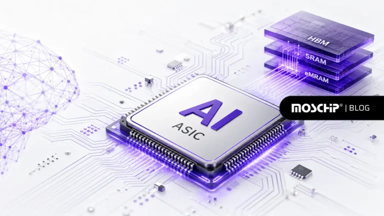
Recently, AI processors have seen significant improvements in computing power due to specialized units such as NPUs…

Text is one of the most important ways humans share information. It gives detailed information. This helps machines understand their surroundings. It…
Android has evolved beyond an operating system into a foundation for building connected, intelligent...
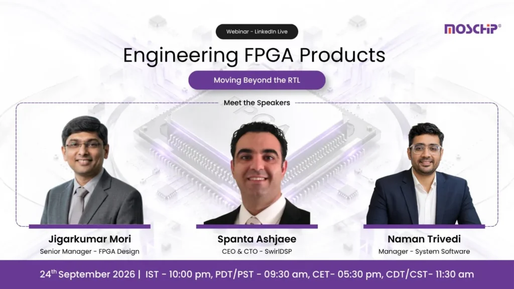
FPGA products are no longer just about getting the RTL right. Building a production-ready FPGA platform...
Today’s consumer products respond after something has happened. Your wearable tells you your heart rate is elevated.…
Designing an FPGA-based product can look straightforward when working within the FPGA development environment…