From RTL to Silicon: A Practical View of the ASIC Design Flow

An electronic system rarely starts in its finished state. They evolve as performance demands increase, requiring technology to manage tighter latency, higher throughput, and more stringent power constraints. General-purpose components start to fall short as these needs increase.
The silicon design is brought into focus by the requirement for efficient, regulated computation, which frequently results in a custom ASIC. This change from architectural intent through design, verification, and implementation to tapeout and manufacturing is outlined in the ASIC design flow.
An ASIC design begins as a defined intent to execute a workload within strict physical limits and ends as a manufactured product operating consistently at scale.
This transition depends on how consistently decisions are carried forward. When early assumptions are inaccurate, the impact appears later, and iterations become costlier.
The need for an ASIC typically arises when a workload exceeds the limits of programmable hardware. Throughput fails to meet required data rates, power consumption exceeds allowable limits, and latency becomes unpredictable under sustained load. At that point, the problem is no longer about flexibility. It becomes a problem of physical efficiency, and a fixed hardware implementation is required.
The ASIC flow translates this requirement into silicon. It begins with defining the physical boundaries, such as specification, architecture, design constraints, and continues through design, validation, manufacturing, and production.
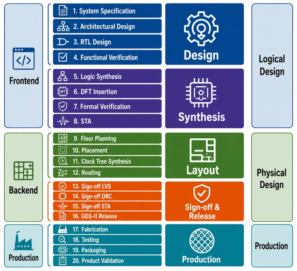
Figure 1: ASIC Design Flow
Selecting a process node establishes the fundamental physical limits within which a chip must operate. Foundries offer various process nodes that dictate critical performance factors, including transistor density, switching speed, and leakage behaviour.
The impact on final performance depends largely on the specific type of node selected.
Crucially, this selection is made before the design process even begins and cannot be altered later. The chosen node permanently defines the chip’s electrical characteristics, its design rules, and the IP blocks. Every subsequent stage of the ASIC design flow, from translating the workload into a structural architecture to final tapeout, must align with the physical boundaries.
Once the process is fixed, the architecture is defined.
The workload is partitioned into hardware and software components. Functions that require deterministic latency or high throughput are implemented in hardware. Functions that benefit from flexibility remain in software.
The architecture defines compute blocks, memory hierarchy, and interconnect structure. Data flow is mapped explicitly, and bandwidth requirements are calculated. Latency is evaluated across each stage.
Performance models are created to estimate throughput, latency, and power. These models serve as a reference. Any deviation observed later can be traced back to assumptions made at this stage.
At this point, the design is fully defined in terms of intent and constraints but not yet implemented. This marks the transition from definition to implementation.
The design flow begins with RTL development and proceeds through each stage to tapeout.
The ASIC design flow is broadly divided into frontend and backend stages. Frontend includes RTL design, verification, and synthesis, focusing on functional correctness. Backend includes DFT, physical design, and signoff, focusing on implementation and manufacturability.
Once the specification and architecture are defined, RTL captures the design in a form that can be realized directly in hardware. It defines data movement, control decisions, and operations across clock cycles.
The implementation is written in hardware descriptive languages (HDL) such as SystemVerilog or Verilog and structured into modules with well-defined interfaces. Each module separates the datapath logic, which performs computation, from control logic, which governs sequencing and state transitions.
Digital hardware operates based on clocks, which act as timing references for all operations. At the RTL stage, designers define how many such clock domains exist and how they interact. When signals move between different clock domains, special synchronization techniques are required to avoid unstable behavior. Similarly, reset defines how the system is brought into a known starting state. This ensures that, when powered on or recovered from an error, the design behaves predictably instead of starting from random values.
Power considerations are also introduced early. One common method is clock gating, where portions of the design are temporarily disabled when not in use, reducing unnecessary switching activity and saving power.
By the end of this phase, RTL provides a complete logical representation of the system, including its structure, timing relationships, and operational behavior.
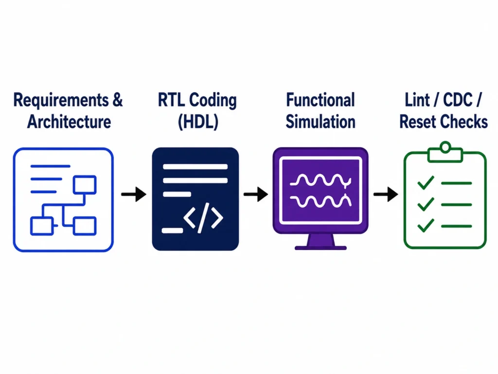
Figure 2: RTL Design and Architecture Flow
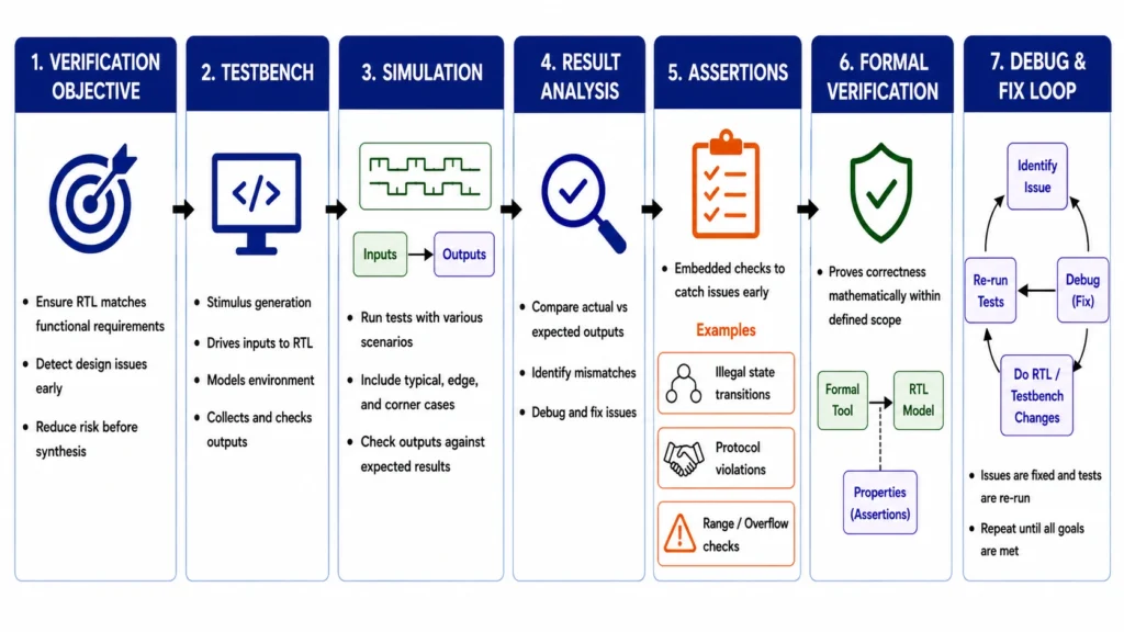
Verification checks whether the RTL behaves as intended under all relevant conditions. The goal is to ensure that the design matches the original functional requirements before moving further in the flow.
This is done through simulation using a range of inputs. These include both typical scenarios and edge cases that may expose corner-case behavior. The resulting outputs are then compared against expected values to confirm correctness.
To understand how thoroughly the design has been tested, coverage metrics are used. Code coverage measures whether all parts of the RTL have been exercised during simulation. Functional coverage, on the other hand, tracks whether all intended behaviors and scenarios have been tested. A mismatch between the two often points to gaps in the verification plan rather than in the code itself.
Assertions are embedded checks that monitor the design during simulation. They help catch issues such as invalid state transitions or protocol violations that occur now, rather than relying only on output comparison.
In addition to simulation, formal verification may be applied to critical blocks. Unlike simulation, which tests selected cases, formal methods attempt to prove correctness across all possible input combinations within a defined scope.
By the end of this stage, the design reaches a level of confidence where its functional behavior is well understood and validated, reducing the risk of costly issues appearing later during physical implementation.
Figure 3: Verification Flow
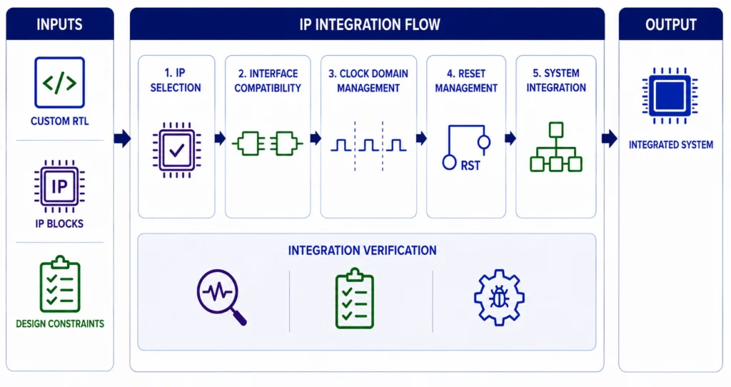
ASIC designs typically combine custom RTL with pre-designed IP block integration.
These IPs include processors, memory controllers, and interface modules. Each IP has defined interfaces, timing characteristics, and configuration requirements.
Integration involves connecting these components into a complete system. Interface compatibility is established in terms of data width, timing, and protocol. Clock domains are aligned, and reset behavior is made consistent.
This stage produces a fully integrated system that behaves as intended under combined operation.
Figure 4: IP Integration and Verification Flow
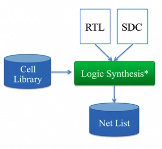
Synthesis converts the RTL description into a gate-level netlist using standard cell libraries specific to the selected process node. This stage translates functional intent into a structurally realizable form while considering timing, area, and power constraints.
Design constraints, typically defined using SDC (Synopsys Design Constraints), guide the synthesis tool in optimizing logic paths to meet target frequency and interface requirements. The generated netlist is evaluated using Static Timing Analysis (STA) to ensure that setup and hold requirements are satisfied under defined conditions.
Basic optimizations such as logic restructuring, buffering, and gate sizing are performed to improve timing and reduce area. Power-aware techniques like clock gating may also be inferred during this stage.
After synthesis, Logical Equivalence Check (LEC) is performed to ensure that the synthesized gate-level netlist is functionally equivalent to the original RTL design. This step is critical to confirm that synthesis optimizations have not altered the intended functionality.
The output of synthesis serves as the input to physical design, making it a critical step where design intent is mapped onto technology-specific implementation.
Figure 5: RTL to Gate-Level Synthesis Flow
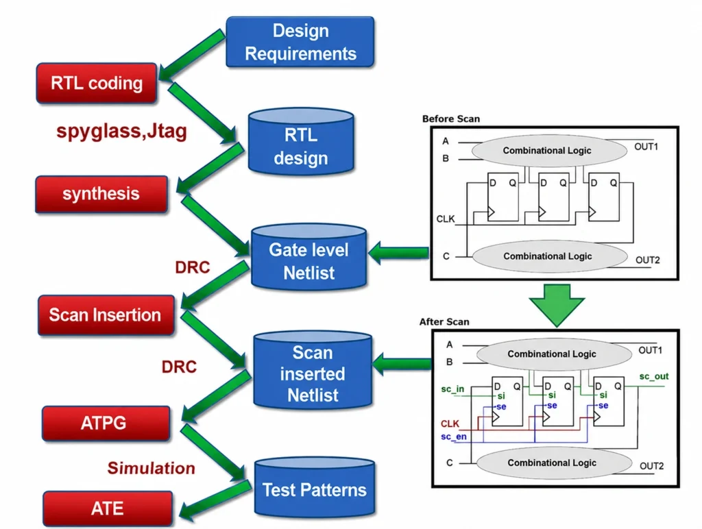
Design for Test (DFT) is introduced after synthesis to ensure that the fabricated chip can be effectively tested for manufacturing defects. At this stage, additional test logic is inserted into the synthesized netlist without altering the functional behavior of the design.
Common DFT techniques include scan chain insertion, where sequential elements are connected to form shift registers, enabling controllability and observability of internal states. Memory structures are augmented with Built-In Self-Test (MBIST) to verify their correctness, while boundary scan (JTAG) facilitates testing of interconnects and external interfaces.
Test coverage is a key metric in this stage, ensuring that a high percentage of possible manufacturing faults can be detected during production testing. The modified netlist generated after DFT insertion serves as the input to physical design, where the added test structures are implemented in the layout.
Advanced techniques such as scan compression and ATPG (Automatic Test Pattern Generation) are used to improve test efficiency and reduce test time during production.
DFT implementation must be carefully coordinated with physical design to minimize routing overhead and timing impact.
Figure 6: DFT Flow
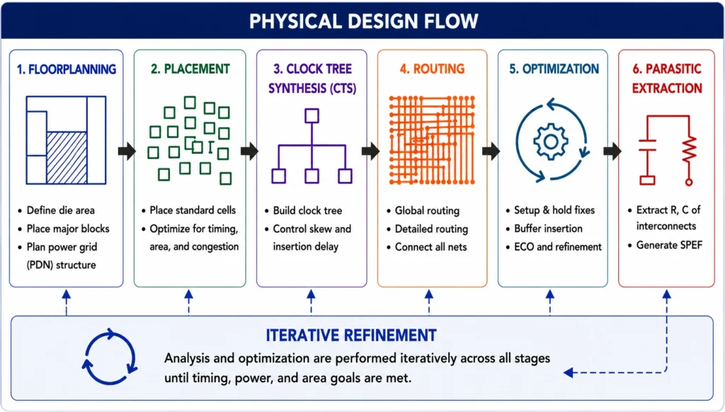
Physical design converts the logical description into a layout that can be fabricated into a real chip.
Physical design begins with the DFT inserted gate-level netlist. The inputs to physical design include the DFT inserted netlist, timing constraints (SDC), standard cell libraries, and physical libraries provided by the target process node. The netlist is evaluated for timing slack, area, and power.
The process follows a structured sequence including floorplanning, placement, clock tree synthesis (CTS), routing, and optimization, with iterative refinement at each stage.
Floorplanning defines the arrangement of major blocks and the structure of the power distribution network.
Placement assigns locations to individual cells, and routing connects them through metal interconnects. After routing, parasitic extraction is performed to model resistance and capacitance of interconnects accurately. These extracted parasitics are used for detailed timing and signal integrity analysis.
Clock tree synthesis distributes the clock signal across the design with controlled timing variation.
Achieving timing closure is a key objective during this stage, requiring iterative adjustments to placement, buffering, and routing to satisfy setup and hold constraints across all defined operating conditions.
Subsequently, timing analysis is performed across multiple process, voltage, and temperature (PVT) corners and operating modes (MCMM) to ensure reliable functionality under all conditions.
Static Timing Analysis (STA) spans both frontend and backend stages, starting from synthesis and continuing through physical design and signoff to ensure timing closure across all operating conditions.
Power integrity analysis identifies voltage drop across the design. Signal integrity analysis evaluates interference between adjacent signals.
The physical design stage produces a layout that satisfies timing, power, and manufacturability requirements. The final layout undergoes detailed verification and signoff checks, including DRC, LVS, STA with extracted parasitics, electromigration (EM), and IR drop analysis, before being approved for tapeout, ensuring all design constraints are satisfied for reliable manufacturing.
Design decisions throughout the flow are driven by trade-offs between performance, power, and area (PPA), which must be balanced based on application requirements.
Figure 7: Physical Design Flow
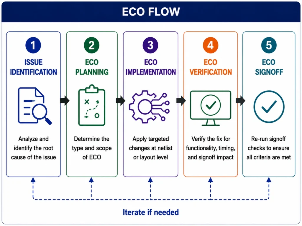
Engineering Change Order (ECO) is used to implement targeted fixes after synthesis or during physical design without requiring a full redesign. ECOs are typically applied to resolve functional issues, timing violations, or late-stage design changes identified during verification or signoff.
Depending on the stage of the design, ECOs may involve modifying logic at the netlist level or making minimal changes at the layout level, such as gate resizing or metal-only modifications. These changes are carefully applied to avoid disturbing the overall design while addressing specific issues.
ECOs may be classified as pre-mask or post-mask (metal ECO), depending on when changes are applied in the manufacturing cycle.
Following ECO implementation, LEC is performed again to verify that the applied changes preserve functional correctness, except for the intended modifications. This ensures that no unintended behavior is introduced during late-stage fixes.
ECOs play a critical role in reducing turnaround time and avoiding costly rework, especially in advanced stages where full re-implementation would significantly impact schedules.
Figure 8: ECO Flow
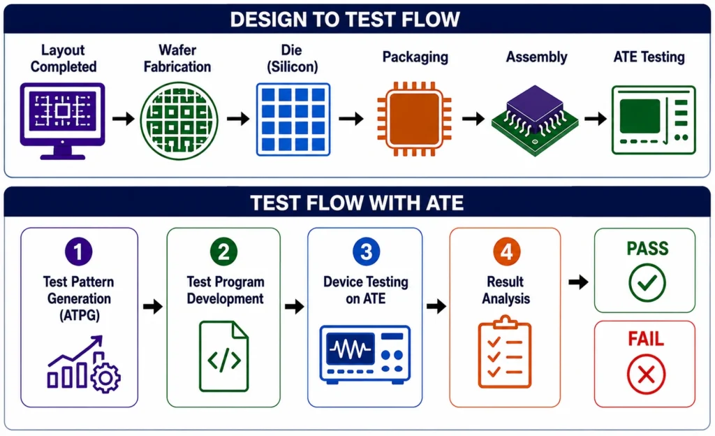
After layout completion, the design is manufactured and assembled.
The silicon die is fabricated using the selected process node and then packaged to provide electrical connections and protection. Packaging influences thermal behavior and signal integrity.
Each unit is tested using Automated Test Equipment (ATE). Test patterns, typically generated using Automatic Test Pattern Generation (ATPG) tools, are applied to achieve high fault coverage and verify functionality and electrical characteristics. ATE testing ensures that each manufactured unit meets defined specifications before further validation.
Figure 9: Package, Assembly, and ATE Testing Flow
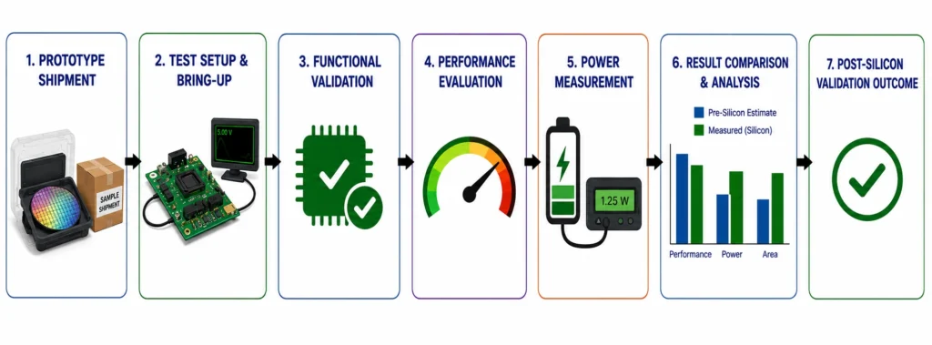
In this stage, the initial silicon samples are evaluated under real operating conditions.
Functional tests confirm that the design behaves as expected. Performance measurements verify throughput and latency. Power is measured under actual workloads.
Measured results are compared with pre-silicon estimates. Differences are analyzed to determine whether they arise from modeling assumptions, physical effects, or integration behavior.
Post-silicon validation provides a confirmed understanding of how the chip behaves in hardware before it proceeds to qualification.
Figure 10: Prototype Shipment and Post Silicon Validation Flow
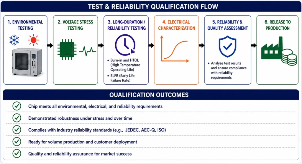
The qualification stage evaluates the chip under environmental and reliability conditions.
Testing includes temperature variation, voltage stress, and long-duration operation. These tests confirm that the design maintains performance and functionality over time.
Successful qualification establishes that the chip meets required reliability standards and is ready for production use.
Figure 11: Qualification and Release to Production
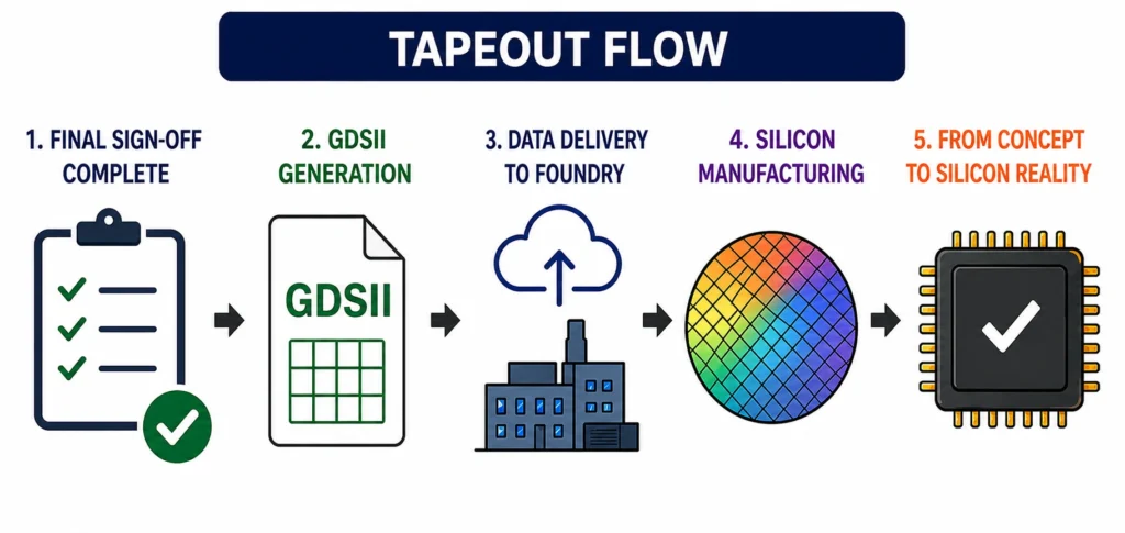
Tapeout marks the point where the design is finalized and released for production.
At this stage, the complete physical layout is delivered to the foundry in the GDSII format, which captures the exact representation of all layers to be fabricated onto the silicon. This data defines the final blueprint of the chip, leaving no scope for further design changes.
With all the stages completed, the ASIC design reaches its final form, transitioning from an engineered concept to a fully realized silicon product.
Figure 12: Tapeout Flow
To conclude, building a custom ASIC involves many interdependent stages, each carrying its own set of constraints and trade-offs. This process begins with defining what the chip must achieve and extends through architecture, implementation, and silicon realization.
The effectiveness of ASIC development lies in how well these stages are structured and aligned. Decisions taken early share the options available later, and misalignment between stages often shows up only when changes become expensive. A disciplined approach across the full flow, supported by domain expertise at each step, helps keep the design stable as it progresses. When executed well, this reduces uncertainty, limits rework, and leads to a more predictable path from concept to working silicon.
MosChip Technologies works across the silicon design and development lifecycle, supporting programs that range from RTL to tapeout with expertise in turnkey ASIC execution, design services – analog/mixed signal design & layout, RTL design & verification, physical design, and IP integration, porting, and customization. MosChip supports designs across process nodes from 180nm to 2nm and is also a TSMC Design Center Alliance (DCA) partner.

Bhanu Prakash Yakkaluri is an RTL Design Manager with over 15 years of experience in ASIC/SoC design and implementation. He has worked on complex HPC processor-based SoCs, including designs based on Arm Neoverse V2. He has contributed across the complete frontend design flow, from micro-architecture to RTL design and functional verification. He has delivered multiple successful tapeouts across technology nodes ranging from 180nm to 5nm. His expertise includes clock and reset architecture, SoC integration, multi-clock domain design, and CDC/RDC analysis. He is proficient in synthesizable RTL design, netlist verification, and automation using Perl scripting. He has strong knowledge of high-speed industry-standard protocols such as IEEE 802.3ae, IEEE 802.11 MAC, and eUSB, AMBA Bus Architectures

Semiconductors sit at the centre of every technology platform. Data centers, automotive, telecom networks, medical systems, and industrial automation rise or fall on silicon capability…

ASIC and SoC verification is the engineering unit responsible for demonstrating that a hardware implementation conforms to its specification across all relevant operating conditions…
Across semiconductor programs, one pattern continues to drain time, predictability, and momentum. Companies don’t fall behind because their architectures are too ambitious…

How can manufacturers transform fragmented operational data into real-time intelligence...

Industrial machines are evolving from systems that simply report their status to system…

The demand for high-bandwidth communication is increasing…