Importance of VLSI Design Verification and its Methodologies
In the dynamic world of VLSI (Very Large-Scale Integration), the demand for innovative products is higher than ever. The journey from a concept to a fully functional product involves many challenges and uncertainties where design verification plays a critical role in ensuring the functionality and reliability of complex electronic systems by confirming that the design meets its intended requirements and specifications. In 2023, the global VLSI market is expected to be worth USD 662.2 billion, according to Research and Markets. According to market analysts, it will be worth USD 971.71 billion in 2028, increasing at a Compound Annual Growth Rate (CAGR) of 8%.
In this article, we will explore the concept of design verification, its importance, the process involved, the languages and methodologies used, and the future prospects of this critical phase in the development of VLSI design.
What is design verification and its importance?
Design verification is a systematic process that validates and confirms that a design meets its specified requirements and sticking to design guidelines. It is a vital step in the product development cycle, aiming to identify and rectify design issues early on to avoid costly and time-consuming rework during later stages of development. Design verification ensures that the final product, whether it is an integrated circuit (IC), a system-on-chip (SoC), or any electronic system, functions correctly and reliably. SoC and ASIC verification play a key role in achieving reliable and high-performance integrated circuits.
VLSI design verification involves two types of verification.
- Functional verification
- Static Timing Analysis
These verification steps are crucial and need to be performed as the design advances through its various stages, ensuring that the final product meets the intended requirements and maintains high quality.
Functional verification: It is a pivotal stage in VLSI design aimed at ensuring the correct functionality of chip used under various operating conditions. It involves testing the design to verify whether it behaves according to its intended specifications and functional requirements. This verification phase is essential because VLSI designs are becoming increasingly complex, and human errors or design flaws are bound to occur during the development process. The process of functional verification in VLSI design is as follow.
- Identification and preparation: At this stage, the design requirements are identified, and a verification plan is prepared. The plan outlines the goals, objectives, and strategies for the subsequent verification steps.
- Planning: Once the verification plan is ready, the planning stage involves resource allocation, setting up the test environment, and creating test cases and test benches.
- Developing: The developing stage focuses on coding the test benches and test cases using appropriate languages and methodologies. This stage also includes building and integrating simulation and emulation environments to facilitate thorough testing.
- Execution: In the execution stage, the test cases are run on the design to validate its functionality and performance. This often involves extensive simulations and emulators to cover all possible scenarios.
- Reports: Finally, the verification process concludes with the generation of detailed reports, including bug reports, coverage statistics, and an overall verification status. These reports help in identifying areas that need improvement and provide valuable insights for future design iterations.
Static Timing Analysis (STA): Static Timing Analysis is another crucial step in VLSI design that focuses on validating the timing requirements of the design. In VLSI designs, timing is crucial because it determines how signals propagate through the chip and affects the overall performance and functionality of the integrated circuit. The process is used to determine the worst-case and best-case signal propagation delays in the design. It analyzes the timing paths from the source (input) to the destination (output) and ensures that the signals reach their intended destinations within the required clock cycle without violating any timing constraints. During STA, the design is divided into time paths so that timing analysis can be performed. Each time path is composed of the following factors.
- Startpoint: The startpoint of a timing route is where data is launched by a clock edge or is required to be ready at a specific time. A register clock pin or an input port must be present at each startpoint.
- Combinational Logic Network: It contains parts that don’t have internal memory. Combinational logic can use AND, OR, XOR, and inverter elements but not flip-flops, latched, registers, or RAM.
- Endpoint: This is where a timing path ends when data is caught by a clock edge or when it must be provided at a specific time. At each endpoint, there must be an output port or a pin for register data input.
Languages and methodologies used in design verification
Design verification employs various languages and methodologies to effectively test and validate VLSI designs.
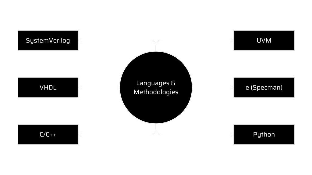
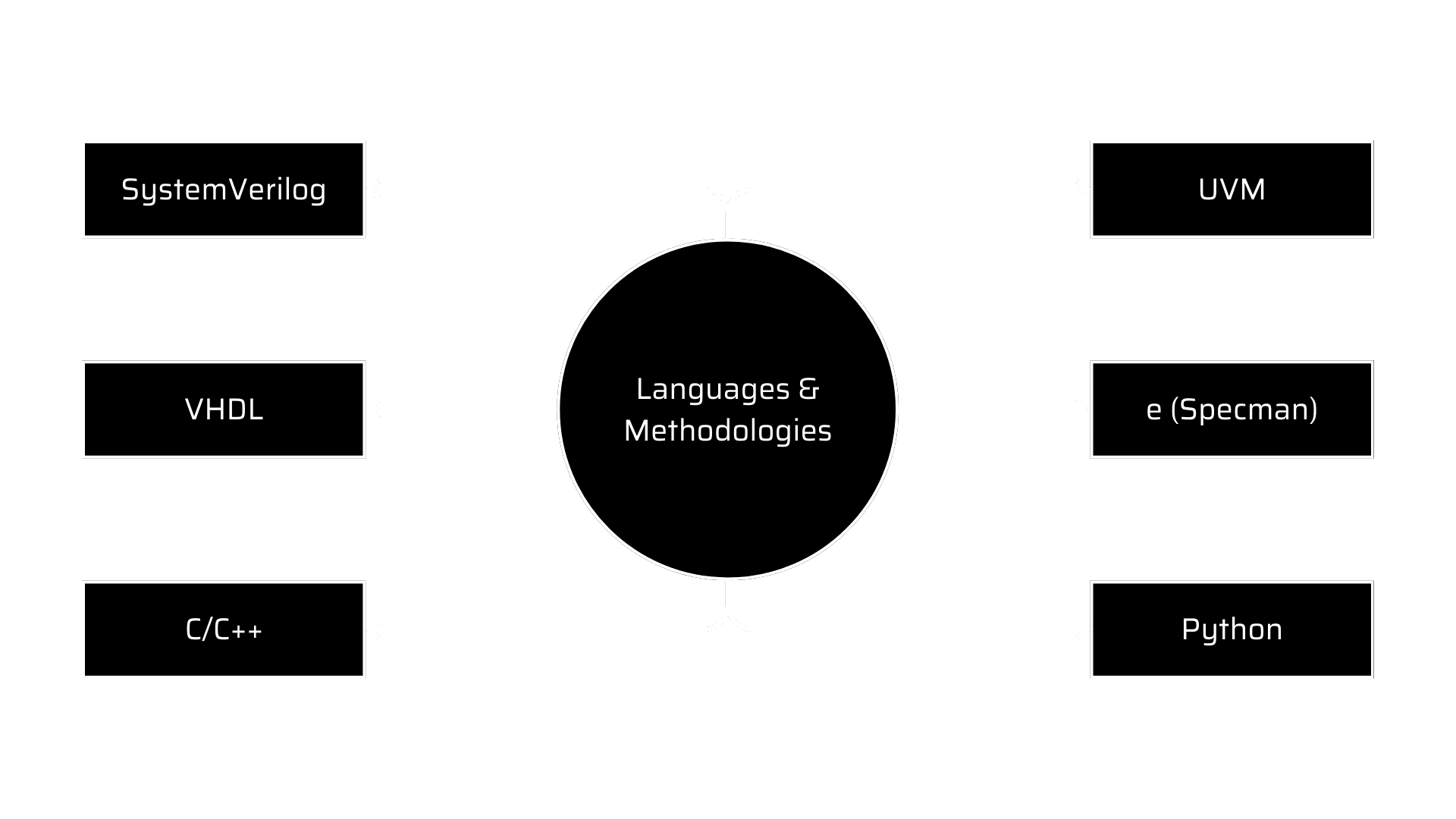
- SystemVerilog (SV) verification: SV provides an extensive set of verification features, including object-oriented programming, constrained random testing, and functional coverage.
- Universal Verification Methodology (UVM): UVM is a standardized methodology built on top of SystemVerilog that enables scalable and reusable verification environments, promoting design verification efficiency and flexibility.
- VHDL (VHSIC Hardware Descriptive Language): VHDL is widely used for design entry and verification in the VLSI industry, offering strong support for hardware modelling, simulation, and synthesis.
- e (Specman): e is a verification language developed by Yoav Hollander for his Specman software that offers powerful verification capabilities, such as constraint-driven random testing and transaction-level modelling. Later it was renamed as Verisity which was acquired by Cadence Design Systems.
- C/C++ and Python: These programming languages are often used for building verification frameworks, test benches, and script-based verification flows.

 VLSI design verification languages and methodologies
Advantages of design verification
Effective design verification offers numerous advantages to the VLSI industry.
- It reduces time-to-market for VLSI products
- The process ensures compliance with design specifications
- It enhances design resilience to uncertainties
- Verification minimizes the risks associated with design failures
The Future of design verification
The future of design verification looks promising. New methodologies with Artificial Intelligence and Machine Learning assisted verification is emerging to address verification challenges effectively. The adoption of advanced verification tools and methodologies will play a significant role in improving the verification process’s efficiency, effectiveness, and coverage. Moreover, with the growth of SoC, ASIC, and low power designs, the demand for specialized VLSI verification will continue to rise.
Design verification is an integral part of the product development process, ensuring reliability, functionality, and performance. Employing various languages, methodologies, and techniques, design verification addresses the challenges posed by complex designs and emerging technologies. As the technology landscape evolves, design verification will continue to play a vital role in delivering innovative and reliable products to meet the demands of the ever-changing world.
At MosChip Company offers a complete range of semiconductor design and verification services, catering to every stage of ASIC/FPGA/SoC development, from initial concept to final deployment. Our highly skilled VLSI team has the capability to design, develop, test, and verify customer solutions involving a wide range of silicon platforms, tools and technology. MosChip also has technology partnerships with leading semiconductor giants like Xilinx, Lattice Semiconductor and Microchip.
About MosChip:
MosChip has 20+ years of experience in Semiconductor, Product Engineering services & Software, security with the strength of 1300+ engineers.
Established in 1999, MosChip has development centers in Hyderabad, Bangalore, Pune, and Ahmedabad (India) and a branch office in Santa Clara, USA. Our software expertise involves platform enablement (FPGA/ ASIC/ SoC/ processors), firmware and driver development, systems security, BSP and board bring-up, OS porting, middleware integration, product re-engineering and sustenance, device and embedded testing, test automation, IoT, AIML solution design and more. Our semiconductor offerings involve silicon design, verification, validation, and turnkey ASIC services. We are also a TSMC DCA (Design Center Alliance) Partner.
Stay current with the latest MosChip updates via LinkedIn, Twitter, FaceBook, Instagram, and YouTube
Author
-

Ambuj is a Marketing professional at MosChip creating impactful techno-commercial writeups and conducting extensive market research to promote businesses on various platforms. He has been a passionate marketer for more than three years and is constantly looking for new endeavours to take on. When He’s not working, Ambuj can be found riding his bike or exploring new destinations.


