FPGA Market Trends With Next-Gen Technology
Due to their excellent performance and versatility, FPGAs (Field Programmable Gate Arrays) appeal to a wide spectrum of businesses. Also, it has the feature of adopting new standards and modifying hardware as per the specific application requirement even after it’s been deployed for usage. ‘Gate arrays,’ on the other hand, relate to the architecture’s two-dimensional array of logic gates. FPGAs are used in several applications where complicated logic circuitry is required and changes are expected. Medical Devices, ASIC Prototyping, Multimedia, Automotive, Consumer Electronics, and many other areas are covered by FPGA applications. In recent years, market share and technological innovation in the FPGA sector is growing at a rapid speed. FPGAs offer benefits for Deep Learning and Artificial Intelligence based solutions, including an improved performance with low latency and high throughput, and power efficiency. According to Mordor Intelligence, the global FPGA market was valued at USD 6958.1 million in 2021, and it is predicted to reach USD 11751.8 million by 2027, with a CAGR of 8.32 percent from 2022 to 2027.
FPGA Design Market Drivers
Global Market Drivers
Let’s look at some interesting real-world applications that can be built using TensorFlow Lite on edge TPU.
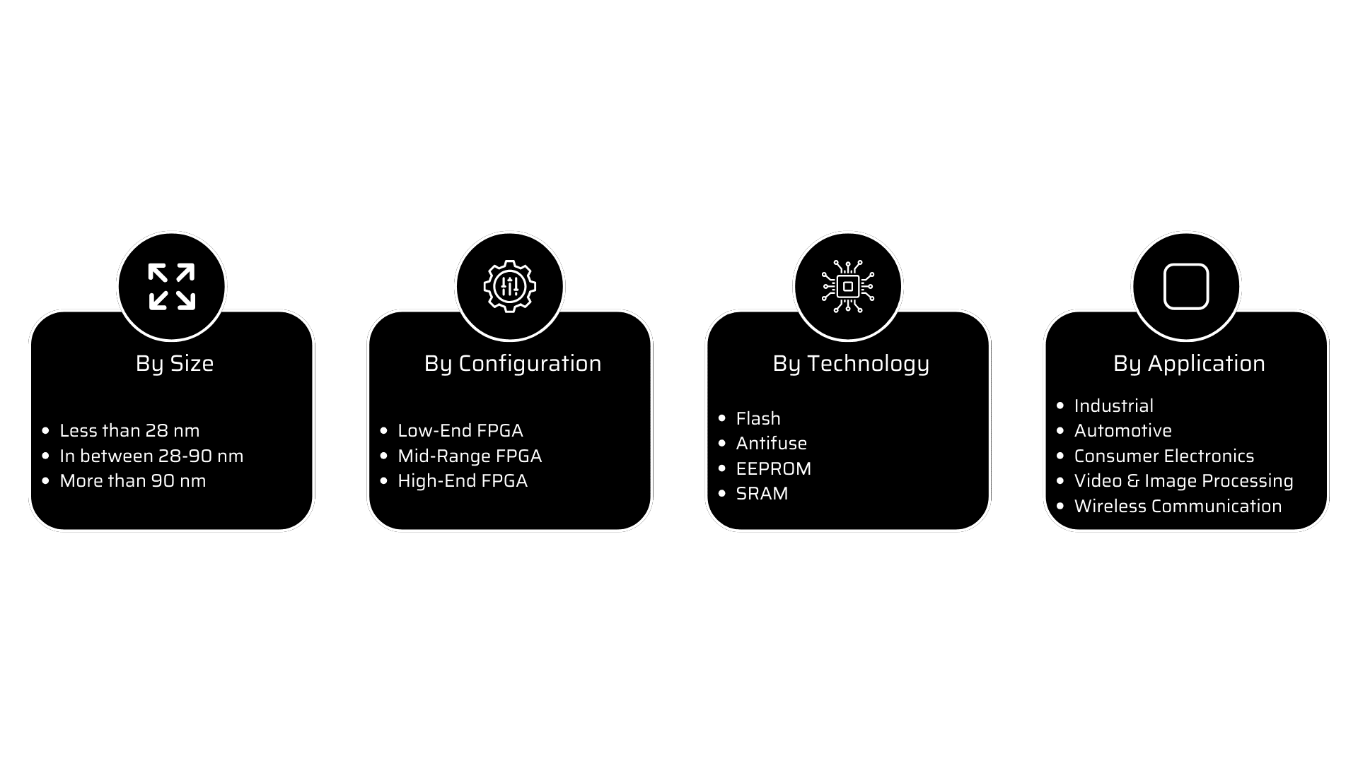
The FPGA market is highly contested due to economies of scale, the nature of product offerings, and the cost-volume metrics favouring firms with low fixed costs. According to the size, 28nm FPGA chips are expected to grow rapidly because they provide high-speed processing and enhanced efficiency. These features have aided its adoption in a variety of industries, including automobiles, high-performance computing, and communications. The consumer electronics sector appears to be promising for FPGA since rising spending power in developing countries contributes to increased market demand for new devices. FPGAs are being developed by market players for use in IoT devices, Natural Language Processing (NLP), based infotainment, multimedia systems, and various industrial smart solutions. Based on the application requirement, either low-end, mid-range or high-end FPGA configurations are selected.
FPGA Architecture Overview
The general FPGA architecture design consists of three types of modules. They are I/O blocks, Switch Matrix, and Configurable Logic Blocks (CLB). FPGA is a semiconductor device made up of logic blocks coupled via programmable connections.
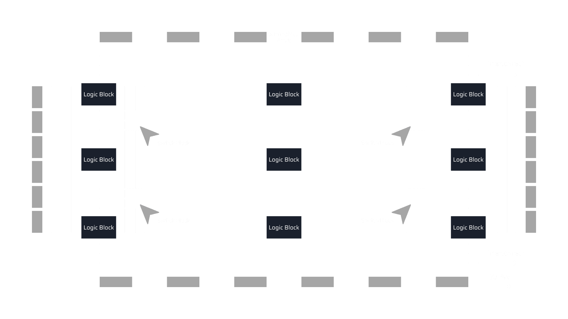
FPGA Architecture
The logic blocks are made up of look-up tables (LUTs) with a set number of inputs and are built using basic memory such as SRAM or Flash to hold Boolean functions. To support sequential circuits, each LUT is connected to a multiplexer and a flip-flop register. Similarly, many LUTs can be used to build for handling complex functions. As per the configurations FPGAs are classified into three types low-end, Mid-end & High-end FPGAs. Artix-7/Kintex-7 series from Xilinx, ECP3, and ECP5 series from Lattice semiconductor are some of the popular FPGA designs for low power & low design density. Whereas Virtex family from Xilinx, ProASIC3 family from Microsemi, Stratix family from Intel are designed for high performance with high design density.
FPGA Firmware Development
Since the FPGA is a programmable logic array, the logic must be configured to match the system’s needs. Firmware, which is a collection of data, provides the configuration. Because of the intricacy of FPGAs, the application-specific purpose of an FPGA is designed using the software. The user initiates the FPGA design process by supplying a Hardware Description Language (HDL) definition or a schematic design. VHDL (VHSIC Hardware Description Language) and Verilog are two commonly used HDLs. After that, the next step in the FPGA design process is to develop a netlist for the FPGA family being used. This is developed using an electronic design automation program and outlines the connectivity necessary within the FPGA. Afterward, the design is committed to the FPGA, which allows it to be used in the (ECB) electronic circuit board for which it was created.
Applications of FPGA
Automobiles
FPGAs in automobiles are extensively used in LiDAR to construct images from the laser beam. They’re employed in self-driving cars to instantly evaluate footage for impediments or the road’s edge for obstacle detection. Also, FPGAs are widely used in car-infotainment systems for reliable high-speed communications within the car. They enhance efficiency and conserve energy.
Tele-Communication Systems
FPGAs are widely employed in communication systems to enhance connectivity and coverage and improve overall service quality while lowering delays and latency, particularly when data alteration is involved. Nowadays FPGA is widely used in server and cloud applications by businesses.
Computer Vision Systems
These systems are becoming increasingly common in today’s world. AI-bots, screen/character readers, and other devices are examples of this. Many of these devices necessitate a system that can detect their location, recognize things in their environment, and people’s faces, and act and communicate with them appropriately. This functionality necessitates dealing with large volumes of visual data, constructing multiple datasets, and processing them in real-time, this is where FPGA accelerates and makes the process much faster.
The FPGA market will continue to evolve as the demand for real-time adaptable silicon grows with next-gen technologies Machine Learning, Artificial Intelligence, Computer Vision, etc. The importance of FPGA is expanding due to its adaptive/programming capabilities, which make it an ideal semiconductor for training massive amounts of data on the fly. It is promising for speeding up AI workloads and inferencing. The flexibility, bespoke parallelism, and ability to be reprogrammed for numerous applications are the key benefits of using an FPGA to accelerate machine learning and deep learning processes.
About MosChip:
MosChip has 20+ years of experience in Semiconductor, Embedded Systems & Software Design, and Product Engineering services with the strength of 1300+ engineers.
Established in 1999, MosChip has development centers in Hyderabad, Bangalore, Pune, and Ahmedabad (India) and a branch office in Santa Clara, USA. Our embedded expertise involves platform enablement (FPGA/ ASIC/ SoC/ processors), firmware and driver development, BSP and board bring-up, OS porting, middleware integration, product re-engineering and sustenance, device and embedded testing, test automation, IoT, AIML solution design and more. Our semiconductor offerings involve silicon design, verification, validation, and turnkey ASIC services. We are also a TSMC DCA (Design Center Alliance) Partner.
Stay current with the latest MosChip updates via LinkedIn, Twitter, FaceBook, Instagram, and YouTube

