Designing mixed-signal and analog ASICs: Engineering considerations and specialized expertise

Every mixed-signal ASIC starts with a simple requirement to convert a physical signal into something a digital system can trust. In practice, that requirement expands into a set of constraints that are tightly coupled and often in conflict.
From an analog design and mixed-signal design standpoint, a mixed-signal ASIC is defined as an end-to-end signal path rather than a collection of independent blocks. Noise, timing, supply, behavior, and layout-induced effects are treated as interdependent variables within the architecture. The objective is not limited to achieving nominal performance, but to ensure that specifications are met consistently across process variation, operating conditions, and layout extracted parasitic effects.
The article examines how those constraints shape the design process, with a focus on signal integrity, architectural trade-offs, and verification strategies required to sustain performance beyond the schematic stage.
Analog circuits process electrical signals that vary continuously in amplitude, frequency, or phase. While digital logic represents information using discrete voltage levels, analog design must preserve subtle variations in signal behavior.
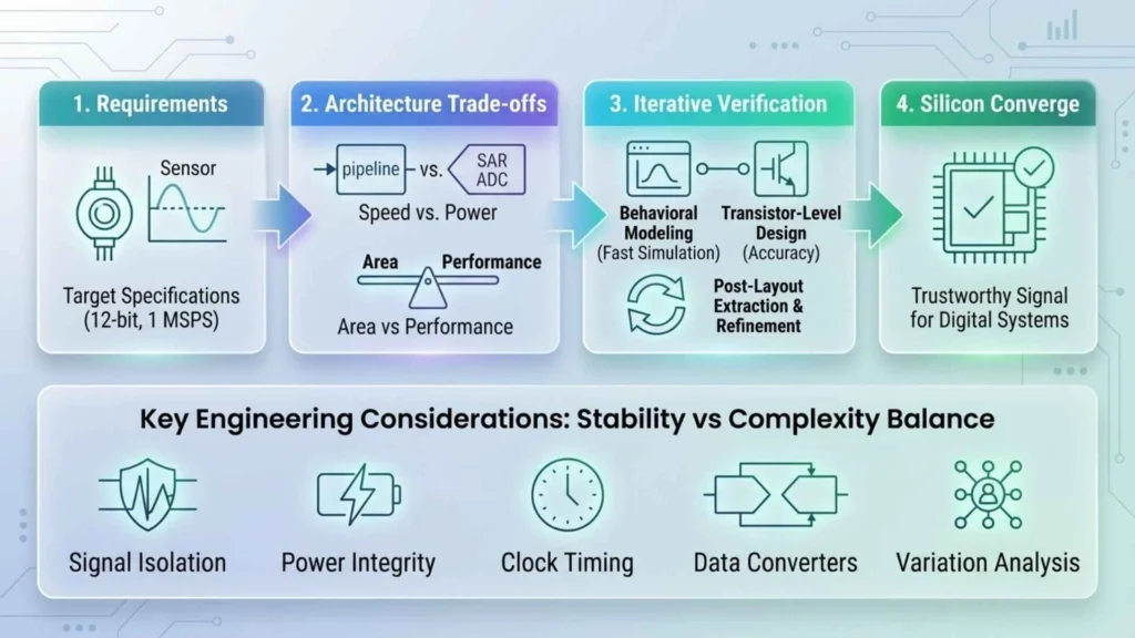
Mixed-signal ASIC design begins with specifications.
A requirement such as “12-bit accuracy at 1 MSPS” is translated into constraint such as noise, floor, linearity, settling time, clock jitter tolerance, reference stability, and power budget. These parameters bound the design space and determine architectural feasibility.
Overview of mixed-signal ASIC design process
Mixed-signal ASICs are used in systems that require precise sensing and control under real-operating conditions. For example, Smart energy meters must measure voltage and current accurately across varying loads while maintaining long-term stability and low power operation.
Better management systems require precise monitoring of cell voltages, current, and temperature across wide operating ranges. These systems must operate reliably under electrical noise and varying thermal conditions.
Industrial sensor interfaces process low-amplitude signals in environments with electromagnetic interference. Signal conditioning must preserve accuracy while enabling real-time digital processing.
Automotive and power electronics systems require mixed-signal ASICs for motor control, power conversion, and system monitoring under demanding electrical and thermal conditions.
Across these applications, analog accuracy defines system limits, while digital logic enables control and communication.
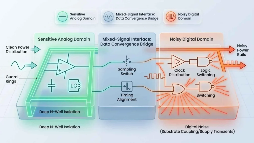
Once analog circuits are placed alongside high-speed digital logic, the design challenge shifts from circuit accuracy alone to system stability. Noise generated by switching logic, power supply transients, and clock distribution effects begins to influence how analog blocks behave on silicon.
Physical Isolation & Noise Management
Integrating analog and digital circuits within the same chip introduces additional complexity. Digital switching noise can couple into analog circuits through the substrate or power network.
Power domain management must ensure stable supply voltages for analog circuits while digital blocks operate with high switching activity. Floorplanning constraints also increase because analog circuits often require symmetric layouts and matched devices.
Many mixed-signal issues do not appear during early simulations. Problems such as substrate noise coupling, power supply fluctuations, and parasitic interactions often emerge only after physical layout and extraction. As a result, mixed-signal development typically involves several iterations between circuit design, layout refinement, and simulation before silicon is finalized.
The demand for mixed-signal ASICs is increasing as systems require tighter integration between sensing, control, and communication.
Smart energy meters, battery management systems, industrial automation platforms, and electric vehicle subsystems all depend on accurate signal conversion and reliable operation under varying conditions.
These applications increase the importance of managing noise, power integrity, and signal accuracy within integrated silicon designs.
MosChip Technologies approaches mixed-signal and analog ASIC development from a system-level perspective, with experience spanning process nodes from 180 nm to advanced 2 nm technologies. This range supports analog-intensive designs on mature nodes as well as high-density integration on advanced processes.
The design methodology integrates analog circuit design, digital ASIC implementation, process-aware development, and silicon validation to maintain correlation from architecture through to silicon. This ensures that mixed-signal systems meet performance, reliability, and integration targets across process variation and operating conditions.

Prasad Motepalli is an experienced Analog and Mixed-Signal design engineer with over 13 years of expertise in analog circuit design, AMS verification, and CAD/EDA flow development. He has worked across advanced semiconductor process nodes including 7nm, 14nm, 22nm, and 180nm technologies from leading foundries.
His technical contributions span a wide range of high-speed and high-performance designs, including SERDES for PCIe and D2D interfaces, GDDR7 memory systems, LPDDR architectures, USB2.0, HDMI, and GPIO libraries. He has hands-on experience in designing critical analog blocks such as delta-sigma ADCs, temperature sensors, calibration circuits, TX drivers, RX slicers, and PLL-related subsystems.
Prasad has led multiple teams in the development of complex IPs and SoCs, contributing to full-chip integration, modeling, and verification methodologies. He has also played a key role in timing library characterization, IBIS model generation, and behavioral modeling using industry-standard tools like Cadence Virtuoso, Liberate, and Spectre. His expertise extends to automation and CAD flow development using SKILL, Python, and shell scripting.
He holds a Master’s degree in VLSI from VEDA-IIT Hyderabad and a Bachelor’s degree in Electronics and Communication Engineering from JNTU, Hyderabad.

The design teams typically invest years and numerous iterations to validate IP and produce a functioning chip. Once this validation is complete, they create derivatives…

Semiconductors sit at the centre of every technology platform. Data centers, automotive, telecom networks, medical systems, and industrial automation rise or fall on silicon capability…

ASIC and SoC verification is the engineering unit responsible for demonstrating that a hardware implementation conforms to its specification across all relevant operating conditions…

For more than five decades, the semiconductor industry advanced along a remarkably predictable path…
Across semiconductor programs, one pattern continues to drain time, predictability, and momentum. Companies don’t fall behind because their architectures are too ambitious…


Know how we have helped our client get more safety rating for their latest auctomobiles launched!