ASIC and SoC Verification: A Comprehensive Methodology Guide

ASIC and SoC verification is the engineering unit responsible for demonstrating that a hardware implementation conforms to its specification across all relevant operating conditions. In modern SoC programs, verification is the primary control mechanism for functional risk, not a post-design validation step.
With each successive process node, chips are becoming more complex, and the cost of a missed bug rises quickly. A defect found after fabrication requires an expensive re-spin and can delay product launch. For this reason, verification serves as the primary method for managing functional risk. It provides clear, measurable evidence that the original architectural intent, the implemented design, and the final system behavior remain aligned from specification to tape-out.
In a typical chip design, verification is treated as a continuous, structured process throughout the entire development cycle. Early planning defines the scope and highlights risk areas. Execution grows as the design matures. Closure is based on defined metrics such as coverage models, assertions, formal checks, and regression quality results. Each stage is intended to reduce uncertainty in a steady and disciplined way.
This article describes a structured, end-to-end verification methodology used in large-scale Full-Custom/Semi-Custom and Chip Design programs. The emphasis is on functional correctness, verification completeness, and repeatability across technology nodes and product generation, showing how verification activities are sequenced, scoped, and measured so that functional risk is systematically reduced and first-pass silicon outcomes become predictable.
Verification is not a later/downstream activity that begins after RTL completion. In ASIC and SoC programs, verification starts during architecture definition and continues through integration, software bring-up, and silicon validation.
When system complexity increases, the dominant sources of functional failure shift away from isolated logic defects toward interactions between subsystems. Clock domain crossings, power management logic, arbitration paths, coherency mechanisms, and software-driven execution sequences account for a large fraction of escaped bugs. A verification methodology must therefore scale with system complexity rather than RTL size.
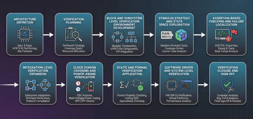
Verification for a complex ASIC or SoC follows a dependency-driven process in which each step establishes the conditions required for the next. Weaknesses introduced early rarely cause immediate failures, but surface later as poor coverage, excessive debug effort, or post-silicon issues.
The flow begins with the definition and verification planning of architectural intent, progresses through block and subsystem-level verification, expands to full-chip and power-aware validation, and concludes with system-level and software-driven verification. Closure is achieved only when coverage goals defined in the verification plan are satisfied across all operating modes and configurations.
ASIC and SoC Verification flow
The steps below describe this flow in sequence.
Step 1: Architectural intent definition
Verification begins with the architecture definition. The objective at this stage is clarity of intent rather than implementation detail. Verification engineers must understand subsystem boundaries, shared resources, concurrency models, configuration space, ordering guarantees, clocks reset behaviour, and power management techniques, native low power techniques, and power down and wakeup/resume analysis/assumptions.
This step establishes where verification depth is required. Control logic, arbitration, coherence, and power management paths are typically identified as high-risk areas. Ambiguity at this stage propagates through the verification process and cannot be corrected later through additional testing. In large-scale ASIC and SoC programs, verification architects participate directly in architecture reviews to capture intent and risk areas before RTL exists.
Step 2: Verification planning and coverage objective definition
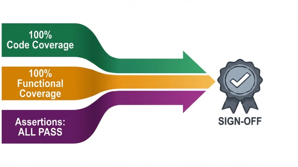
Architectural intent is translated into a verification plan that establishes traceability between the specification and verification actions. For each architectural feature, the plan defines how correctness will be demonstrated and how completeness will be measured by a goal of achieving 100% functional and code coverage.
Coverage objectives are defined early to avoid subjective closure decisions. The verification plan constrains all subsequent activities. Verification environments, stimulus strategies, and metrics must align with it. In large Custom/Semi-Custom Chip Design programs, static or incomplete plans are a common source of escaped functional bugs.
Step 3: Block and subsystem-level verification environment development
With the verification plan in place, verification environments are developed at the block and subsystem level. The objective is isolation, early validation, and reuse.
Subsystem-level environments allow verification logic to be developed and debugged before full-chip integration. Transaction-level abstraction is used to express stimulus and checking in architectural terms rather than signal activity. Reference models and checkers are introduced where architectural comparison is required.
Verification assets developed at this stage are later reused during higher levels of integration with minimal modification.
Step 4: Stimulus strategy and state space exploration
Once block and subsystem-level verification environments are structurally complete, stimulus strategy becomes the primary focus. At this stage, environments include stable protocol-aware drivers, monitors, checkers, or scoreboards, and functional coverage models aligned to the verification plan. These environments allow stimulus to be expressed at the transaction level, with protocol handling and checking abstracted away from individual tests.
Directed stimulus is first used to validate expected behaviors, configuration paths, and basic functionality within these environments. Once baseline correctness is established, constrained random stimulus is introduced to explore legal but non-obvious combinations of events, timing relationships, and shared resource contention. Constraints encode architectural legality, while functional coverage feedback guides refinement of stimulus to expose unexercised interaction scenarios.
Step 5: Assertion-based checking and localized failure detection
Functional Checkers/Assertions need to be implemented to verify the designer’s intent of the implementation with respect to the specification. Assertions are deployed alongside stimuli to detect violations close to their source. They formalize protocol rules, sequencing constraints, and safety conditions derived from architectural intent.
Assertion-based checking changes the nature of debugging. Instead of detecting failures at outputs and tracing backward, violations are flagged at the point where intent is broken. Assertions also act as executable documentation of design assumptions.
At this stage, assertion placement and coverage are reviewed to ensure that critical paths are adequately monitored.
Step 6: Integration-level verification expansion
As verified subsystems are integrated, the scope of verification expands to system-level architectural behavior. The focus shifts to validating interactions between subsystems, shared resource arbitration, ordering guarantees, and interconnect correctness under concurrent operation.
Traffic from multiple interfaces is applied simultaneously, increasing concurrency and contention on shared resources such as interconnects, buffers, and control logic. The objective is to confirm that subsystems which function correctly in isolation continue to behave correctly when operating together, and that architectural assumptions hold under realistic interaction and load conditions.
Step 7: Clock domain crossing and Power-aware verification
Integration introduces additional timing and power-related state dimensions that must be verified explicitly. Clock domain crossings are validated through a combination of structural analysis, CDC-specific protocol checking, and formal techniques to ensure correct synchronization, data transfer, and control behavior across asynchronous boundaries.
Power-aware verification exercises isolation, retention, and state restoration logic during power state transitions that occur while functional activity is ongoing. These scenarios validate that architectural state is preserved and restored correctly when power domains are gated, re-enabled, or sequenced dynamically.
CDC and power-related behaviors are orthogonal to functional stimulus because failures arise from asynchronous timing relationships and power state changes rather than incorrect transaction sequences. These issues often escape earlier verification stages and are a common source of silicon-only failures when not addressed systematically.
Step 8: Static and Formal verification application
Static and formal verification techniques are applied selectively to design regions where exhaustive simulation is impractical or insufficient. These techniques are most effective for control logic, state machines, arbitration paths, clocking-related control, and safety-critical conditions with well-defined intent.
Formal verification complements simulation by proving properties across all legal state combinations within explicitly defined architectural bounds. Rather than replacing simulation, it is used to close coverage gaps in areas where random or directed stimulus cannot reliably reach rare or corner-case scenarios.
When full formal analysis is not tractable, hybrid approaches combine simulation-derived constraints, abstraction, and targeted formal properties to manage state space complexity. Applied in this manner, formal methods significantly increase confidence in critical logic where simulation coverage is inherently limited.
Step 9: Software-driven and system-level verification
As the design reaches functional and interface stability, software execution is introduced into the verification flow. Software-driven scenarios exercise architectural behavior over long execution sequences, enabling validation of cross-subsystem interactions, control paths, and state evolution that cannot be observed through transaction-level tests alone.
These scenarios may be executed using ESL models, virtual platforms, acceleration, or emulation, depending on design maturity and execution requirements. The objective is to validate end-to-end system behavior as visible to software, rather than isolated transactions, and to ensure that hardware and software assumptions remain consistent before silicon.
Step 10: Verification closure and sign-off
Verification concludes when the coverage objectives defined in the verification plan are satisfied across all operating modes, configurations, and power states. Verification artifacts are the documented outputs of the verification process, including plans, environments, assertions, coverage models, reports, and sign-off summaries, that provide traceable and reviewable evidence of verification completeness.
Verification Closure and Sign-off
Closure is determined by measurable verification results aligned to architectural intent, not by regression pass counts or test volume. Verification artifacts, coverage data, and identified limitations are reviewed as part of formal sign-off. At this stage, any remaining functional risk is explicitly understood, documented, and accepted based on objective evidence.
Together, these steps describe a verification methodology that progresses from architectural intent definition through increasing levels of integration, system realism, and objective closure. Each stage builds on the previous one, with verification scope and coverage criteria defined early and validated continuously through sign-off.
In Turnkey ASIC and SoC projects, verification provides a common execution framework across teams, schedules, and ownership boundaries. The verification plan and coverage objectives act as the binding contract between architecture, RTL development, and verification, allowing work to proceed in parallel without relying on informal assumptions or late integration discovery.
Verification environments established early in the program are reused across RTL drops to validate correctness as functionality is implemented. Directed tests and assertions are applied to stabilize new logic and enforce architectural rules at the point of implementation. This execution model enables rapid fault isolation and limits integration risk in multi-site and distributed delivery programs.
As integration progresses, constrained-random stimulus and functional coverage are used to assess interaction depth across shared resources, concurrency paths, and ordering behavior. Coverage data provides objective visibility into verification progress and remaining risk, supporting informed decisions during integration reviews and sign-off preparation. Regressions serve to preserve verified behavior across RTL updates rather than to indicate verification completeness.
Verification closure is determined by coverage satisfaction against the agreed plan, with a goal of 100% functional and code coverage.
Verification artifacts provide traceable evidence suitable for handoff, audit, and silicon sign-off. This model supports predictable delivery in Turnkey ASIC programs by making verification status measurable, reviewable, and independent of individual test interpretation.
This methodology serves as a practical reference for teams responsible for delivering production silicon, where verification quality is measured by what can be proven and signed off, not by what is assumed to work.
MosChip Technologies supports ASIC and SoC programs across the silicon design and development lifecycle, including Turnkey ASIC engagements spanning RTL implementation, verification, physical design, and volume production. It has executed analog and mixed-signal design, along with taking care of physical design, and offers IP integration, porting, and customization. The silicon engineering teams operate within structured, coverage-driven methodologies aligned to production sign-off requirements. MosChip supports designs across 180nm to 2 nm process technologies, ranging from mature nodes to advanced nodes, and is a TSMC Design Center Alliance (DCA) partner.

Ramakrishna Reddy Amudalapati has more than 20 years of experience in ASIC, IP, and SoC design verification, along with substantial work in functional verification, production test vector development, and execution. His expertise spans multiple ASICs and SoCs, covering complete verification cycles at RTL, gate level, and post-layout stages, followed by production test vector development and validation. His technical background includes deep familiarity with multiple protocols, including USB 1.1, USB 2.0, USB 3.0, PCIe, SATA, HDCP, HDMI, and 10/100 Ethernet protocols.
Ramakrishna has led verification architecture and micro-architecture development and has designed a wide range of functional models, including USB host, hub, and device controller BFMs, UTMI-based OTG and UVC models, HDMI-HDCP models, and a PCIe-to-display controller model. His expertise also includes RTL design for the OHCI master and slave operational blocks and the HDMI-Rx HDCP authentication logic. He has overseen functional production test vector development and coverage analysis across several ASIC programs such as MCS7710/11/15/20, MCS7780/7784, MCS7830, MCS9735, and MCS9950.
Across semiconductor programs, one pattern continues to drain time, predictability, and momentum. Companies don’t fall behind because their architectures are too ambitious…

Every mixed-signal ASIC starts with a simple requirement to convert a physical signal into something a digital system can trust…

Semiconductors sit at the centre of every technology platform. Data centers, automotive, telecom networks, medical systems, and industrial automation rise or fall on silicon capability…

For more than five decades, the semiconductor industry advanced along a remarkably predictable path…


Know how we have helped our client get more safety rating for their latest auctomobiles launched!