Advancing Technology Nodes: The Era of Divergent Scaling

For more than five decades, the semiconductor industry advanced along a remarkably predictable path. Moore’s Law guided transistor scaling, while Dennard scaling ensured that reducing dimensions automatically delivered improvements in performance, power efficiency, and density. Each new technology node brought faster transistors, lower operating voltages, reduced interconnect delay, and higher integration density.
During this period, physical design and custom chip design flow benefited enormously from scaling. As transistors became smaller, interconnects naturally shortened. Timing improved almost automatically, power density remained manageable, and routing complexity was largely proportional to design size. The role of physical design focused on optimization rather than limitation.
In early CMOS generations, technology node names had direct physical meaning. A 180nm or 65nm process accurately reflected gate length or metal pitch. Shrinking geometry improved nearly every aspect of chip behaviour in unison.
This predictable relationship began to weaken as the industry approached the 28nm node. At around 28 nm, planar CMOS scaling encountered fundamental physical barriers. Short-channel effects intensified, leakage currents rose sharply, and process variability became increasingly difficult to control. Further reductions in channel length no longer produced proportional performance gains.
From this point forward, technology node names transitioned from physical measurements to generational labels. Although nodes such as 7nm, 5nm, 3nm and 2nm suggest aggressive shrinkage, the actual physical gate lengths changed only modestly. Gate lengths that were already close to 30 nm at 28 nm reduced to around 18 to 20nm at 7nm, and approximately 10 to 12 nm at 5 nm. Beyond this, scaling slowed dramatically.
Yet transistor density continued to increase. This was made possible by a fundamental shift from geometric scaling to architectural scaling.
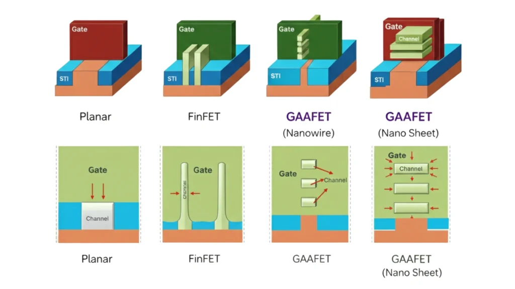
The industry moved away from planar MOSFETs and introduced three-dimensional transistor structures that enhance electrostatic control and current drive without aggressive channel length reduction. This shift fundamentally changed the meaning of scaling.
The first major architectural breakthrough was the FinFET. Instead of forming the transistor channel horizontally on the substrate, FinFETs introduced a vertical silicon fin around which the gate wrapped on three sides. This structure significantly improved electrostatic control over the channel.
FinFET technology enabled lower leakage, reduced short-channel effects, and better performance at reduced voltages. It successfully extended CMOS scaling from the 22nm node through the 7nm generation and became the industry standard for nearly a decade.
However, FinFET scaling eventually reached its own limits. As fins became narrower, carrier mobility degraded, and variability increased. Increasing fin height introduced mechanical and manufacturability challenges, while adding more fins resulted in quantized transistor sizing that limited optimization flexibility. As gate lengths continued to shrink, the electrostatic advantage of the fin structure also began to erode.
These limitations made it clear that simply refining FinFETs was no longer enough. Continued scaling demanded a stronger form of gate control, paving the way for GAAFET architectures as the next major transistor transition.
Gate-all-around transistors represent the strongest electrostatic architecture achievable in silicon. In these devices, the gate fully surrounds the channel, eliminating leakage paths and significantly improving short-channel behaviour.
Rather than using a single vertical fin, GAAFETs form the channel using stacked horizontal silicon structures. This enables current drive to scale vertically instead of laterally, allowing density improvement without aggressive channel length reduction.
Early GAAFET implementations used nanowires, extremely thin silicon channels offering excellent gate control and ultra-low leakage. While electrically robust, nanowires suffered from limited drive current due to their small cross-section, making them less suitable for high-performance logic.
This led to the adoption of nanosheet transistors. Nanosheets replace thin wires with wider horizontal silicon sheets stacked vertically. Their adjustable width restores transistor sizing flexibility and enables significantly higher drive current. Modern 3-nanometer and beyond technologies rely primarily on nanosheet GAAFETs.
Through this architectural transition, transistor performance and density continue to improve even though physical gate length scaling has nearly plateaued.
While transistor innovation has advanced through three-dimensional architecture, interconnects have not experienced a comparable transformation. Metal wires remain fundamentally planar conductors whose electrical behaviour continues to depend almost entirely on geometric shrink. To accommodate rising transistor density, each successive technology node reduces wire width, spacing, and metal pitch. Although this shrink remains manufacturable, it introduces severe electrical penalties that worsen with every generation.
To partially compensate for routing demand, advanced processes have expanded the number of routing layers through increasingly complex multi-level metal stacks. Modern nodes may employ more than fifteen metal layers, with lower layers optimized for dense local routing and upper layers reserved for long global connections and power distribution. While taller metal stacks improve routing reach, they do not improve the electrical quality of the wires themselves. Lower metal layers become extremely narrow and resistive, while upper layers consume significant process cost and are limited in availability, forcing most signals to remain confined to degraded lower metals.
At the same time, aggressive pitch scaling has exceeded the resolution limits of optical lithography, requiring double and multi-patterning techniques to define fine metal geometries. Although double patterning enables continued dimensional shrink, it introduces new constraints such as restricted routing directions, minimum coloring rules, cut-mask dependencies, and overlay sensitivity. These patterning requirements reduce effective routing flexibility and often lower usable track density well below theoretical values, further amplifying congestion, and layout complexity.
As wire dimensions continue to decrease, the conductive cross-section shrinks rapidly while barrier and liner layers occupy an increasing fraction of the metal volume. Electron surface scattering and grain-boundary effects further degrade conductivity. As a result, wire resistance rises sharply, increasing faster than geometry scaling alone would predict. In many advanced nodes, even short local interconnect segments contribute significant delay.
Simultaneously, shrinking wire spacing causes coupling capacitance to dominate over ground capacitance. Signal delay becomes increasingly dependent on neighboring switching activity rather than simply on wire length. Timing behavior becomes context-dependent, introducing variability that cannot be captured by static topology alone and significantly complicating closure.
Together, these effects mark one of the most important transitions in modern semiconductor design. While transistors continue to scale beneficially through architectural innovation, interconnects rely on geometric shrink, patterning complexity, and taller metal stacks that collectively degrade electrical behavior. As a result, transistor scaling remains constructive, while interconnect scaling has become fundamentally destructive.
As transistor density continues to increase, routing congestion has undergone a fundamental transformation. Congestion is no longer merely a placement problem but an inherent property of advanced technology nodes, directly impacting custom chip design and RTL-to-GDSII implementation flows. Complex multi-patterning rules, restrictive via configurations, limited routing directions, and severely constrained pin accessibility significantly reduce effective routing capacity. As a result, even designs with moderate utilization can become unrouteable due to localized routing demand from clock networks, power grids, and high-activity nets. What was once considered an implementation inefficiency has now become an intrinsic characteristic of advanced nodes.
At the same time, shrinking wire dimensions operate at extremely high current densities, causing reliability to emerge as a first-order constraint in modern implementation. Electromigration limits now impose minimum width requirements on many critical nets, particularly clock signals and high-frequency data paths. Buffer insertion intended to improve timing increases switching current and further worsens electromigration stress, causing timing optimization and reliability optimization to frequently oppose one another. Alongside lifetime physics, manufacturability has also become a dominant concern. Aggressive pitch scaling, tight enclosure margins, complex via structures, and pattern-dependent effects introduce strong Design-for-Manufacturability sensitivity, where small geometric variations can translate into large resistance and reliability shifts. As a result, physical implementation is no longer governed solely by geometric design rules, but increasingly by a combination of lifetime physics, process variability, and DFM robustness constraints.
With continued scaling, coupling capacitance has come to dominate interconnect behaviour, meaning that signal integrity has evolved from a localized issue into a structural property of the routing fabric. Crosstalk-induced delay variation, increased noise susceptibility, and data-dependent timing behaviour emerge across entire routing regions rather than in isolated hotspots. Mitigation techniques such as increased spacing and shielding may reduce noise locally, but they consume valuable routing resources and intensify congestion elsewhere. Signal integrity is no longer an exception to be fixed late in the flow; it is embedded into the structure of advanced-node interconnects.
These limitations become most visible in the clock network, where clock routing exposes the practical limits of interconnect scaling. Clock signals traverse the entire die, switch continuously, and must satisfy extremely tight skew and jitter constraints. To remain reliable, clock nets require wide metal geometries, large spacing, and preferential access to upper routing layers. These requirements consume a disproportionate amount of routing capacity and often determine whether a floorplan is feasible at all.
As density continues to rise, a growing fraction of chip area and power is consumed not by logic, but by supporting infrastructure. Repeaters, clock buffers, shielding wires, and wide reliability-safe routing increasingly occupy silicon that would otherwise contain functional circuitry. This infrastructure overhead expands with each technology generation, reducing the effective logic density that scaling is expected to deliver.
In parallel, dynamic power progressively shifts from computation to interconnect switching. More energy is spent moving signals across resistive and capacitive wires than performing logical operations. As a result, performance gains flatten despite faster transistors, and improvements in power efficiency slow dramatically.
Together, these effects explain why timing closure has become one of the most difficult challenges at advanced nodes, even as transistor performance continues to improve on paper. In many modern designs, the ability to route the clock network cleanly, reliably, and within electromigration limits ultimately defines the upper bound of achievable operating frequency.
As interconnect limitations intensified, the industry was compelled to move beyond incremental process tweaks and adopt structural solutions. One of the most significant responses is Backside Power Delivery, where power routing is shifted to the backside of the wafer. By physically separating power distribution from signal routing, this approach reduces competition for routing resources, shortens power delivery paths, lowers IR drop, and substantially relieves congestion in the front-side metal layers.
Another major development is Three-Dimensional Integration. By stacking dies vertically or integrating logic and memory through high-density interconnects, the average wirelength within a system is reduced dramatically. Signals that would otherwise travel across millimeters of horizontal metal routing can instead be exchanged through micrometer-scale vertical connections, leading to meaningful improvements in both performance and power efficiency.
Equally critical is Design-Technology Co-Optimization, which aligns transistor architecture, standard-cell layout, metal stack configuration, and routing rules around realistic design requirements. Parameters such as cell height, pin accessibility, routing directionality, and layer utilization are no longer defined independently, but are co-developed to reduce interconnect stress and improve overall wiring feasibility.
These innovations are not primarily intended to make transistors switch faster. They exist to ensure that transistors can communicate effectively.
Conclusion
The idea of scaling has not disappeared; it has simply grown more complex.
Progress is no longer driven by uniform shrink or automatic gains, but by how well constraints are understood, balanced, and absorbed into design choices. As physical limits become more visible, advancement depends less on pushing dimensions further and more on shaping complexity into something sustainable.
The trajectory forward is not defined by a single breakthrough, but by many quiet adjustments, architectural shifts, structural refinements, and deliberate compromises that together preserve momentum.
In this landscape, improvement is measured not by how far boundaries are pushed, but by how effectively they are navigated.
Scaling continues, not as a race toward smaller numbers, but as an evolving dialogue between what physics allows and what engineering enables.
MosChip, with its deep expertise in the Physical Design domain, supports advanced-node custom silicon development through disciplined RTL-to-GDSII execution that addresses interconnect, power, and reliability constraints from the outset. The company delivers congestion-aware floorplanning, timing-driven placement and routing, robust clock, and power network design, and thorough electromigration, IR-drop, and signal-integrity signoff, combined with design-technology co-optimization to ensure layouts remain routable, manufacturable, and predictable.

Raghuveer serves as a Manager, Physical Design at MosChip Technologies Ltd. He holds a Post Graduate degree from JNTU University, Hyderabad, with over 14 years of industry experience across 64 nm, 28 nm, 14 nm, 10 nm, 7 nm, 5 nm, and 3 nm technology nodes. Has delivered complex semiconductor designs from early implementation through final signoff across multiple product cycles. His expertise centres on Physical Design and signoff, with a proven track record in resolving critical timing challenges, navigating dense interconnect constraints, and driving convergence across performance, power, and yield for both wire-bond and flip-chip design methodologies.

ASIC and SoC verification is the engineering unit responsible for demonstrating that a hardware implementation conforms to its specification across all relevant operating conditions…

Every mixed-signal ASIC starts with a simple requirement to convert a physical signal into something a digital system can trust…

The explosion in computational complexity, networking speeds, and Artificial Intelligence is fundamentally reshaping the semiconductor industry…

Semiconductors sit at the centre of every technology platform. Data centers, automotive, telecom networks, medical systems, and industrial automation rise or fall on silicon capability…
You must be logged in to post a comment.


Know how we have helped our client get more safety rating for their latest auctomobiles launched!
“A sharp and realistic articulation of post-28nm scaling challenges. The distinction between constructive transistor evolution (FinFET to GAAFET) and destructive interconnect scaling is very well captured. The emphasis on clock network limits, EM constraints, coupling-driven delay variability, and routing congestion reflects true implementation experience. Particularly appreciate the clarity around infrastructure overhead redefining effective density. Well written and technically grounded.”
Thank you for the thoughtful note. Much of the constraint now lives in clocking, EM margins, SI, and routing, so it is good to know that perspective resonated. I am glad the implementation realities behind scaling came through clearly.