
The Complete Guide to Silicon Design and Development Services
Semiconductors sit at the centre of every technology platform. Data centers, automotive, telecom networks, medical systems, and industrial automation rise or fall on silicon capability. Software defines features, but the silicon defines limits. Once those limits are set, every other engineering decision must fit inside them.
As systems grow more complex, chips carry far more architectural responsibility than before. Compute models, thermal and power limits, safety boundaries, and product roadmaps are now aligned with chip design fixed before release. Silicon stops being a component and becomes infrastructure.
The scale of this shift is clear. In 2024, the global semiconductor market reached USD 681.05 billion. It grows to USD 755.28 billion in 2025 and is projected to reach USD 2,062.59 billion by 2032, at a 15.4 percent Compound Annual Growth Rate (CAGR), according to Fortune Business Insights. This growth does not come from incremental device upgrades. It comes from deeper silicon integration across every product category that now depends on compute, connectivity, monitor, and control. At this scale, silicon decisions shape the entire product stack. Silicon design and development services move from supporting roles into the core of technology execution, especially in programs that adopt a Turnkey ASIC approach to carry intent from specs to volume production.
This guide explains how the semiconductor ecosystem works and what it takes to move from concept to silicon production.
Why is custom semiconductor design growing?
Custom chip design follows a predictable pattern inside product companies. Teams start with standard components and discover bottlenecks only after system integration begins. By then, architectural choices already limit performance, power, and verification scope.
Modern workloads focus more on data movement than processing, and general-purpose architectures struggle to optimize for this imbalance. Custom designs adapt memory hierarchies and interconnect paths to fit actual system behavior. Also, when the integration density increases, the complexity of verification also rises due to subsystem interactions. Fixed-function silicon requires validation of unused behaviors and obscures critical paths, while Custom Silicon designs streamline validation to essential product features.
The semiconductor design ecosystem
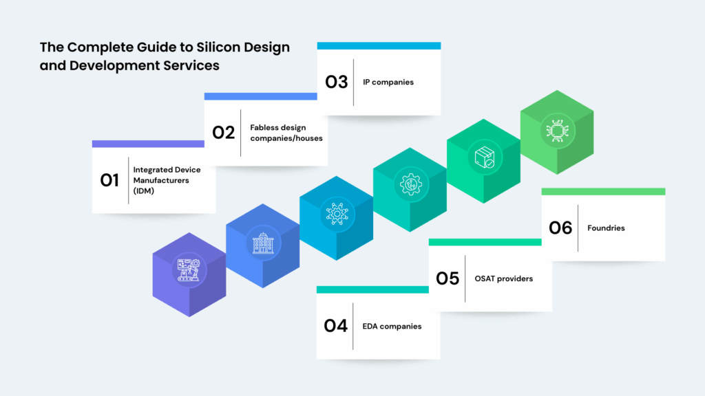
The semiconductor industry functions much like a tightly coupled ecosystem. Each participant specializes in a specific stage, like design, manufacturing, assembly, and testing, all of which are interdependent. At a high level, the industry can be grouped into several distinct company types, each defined by the scope of responsibility they assume.
These roles span Integrated Device Manufacturers (IDM), fabless companies, foundries, silicon design houses, IP companies, EDA companies, and OSAT providers. Each contributes a focused capability rather than owning the entire flow end-to-end. Most commercial programs combine several of these players within a single development effort. Together, they form the operational backbone of semiconductor development.
The roles of these participants can be summarized as follows:
- Integrated Device Manufacturers (IDMs): Manufacture components/wafers for the silicon, aligning with process technology.
- Fabless design companies/houses: Design and develop a chip by defining specs, architectures, and developing silicon based on customer requirements, and do a foundry hand-off.
- IP companies: Develop and license reusable design blocks such as processor cores, interfaces, and interconnects.
- EDA companies: Build tools that enable design, verification, physical implementation, and sign-off.
- OSAT providers: They handle packaging, assembly, and final testing for the silicon.
- Foundries: Manufacture silicon based on customer designs. Foundries provide process technologies, PDKs, design rules, and yield optimization to enable manufacturable and high-performance chips at scale.
The semiconductor design ecosystem
Nowadays, AI and RISC-V increasingly shape how silicon gets defined and built. AI introduces new demands on data movement, memory behavior, and power control. At the same time, RISC-V offers an open and modular instruction set architecture that allows architects to extend and tailor cores for specific workloads. As a result, silicon design service providers in the ecosystem play a direct role in turning AI requirements and RISC-V flexibility into viable chip architectures.
What semiconductor design service providers do?
Semiconductor design service providers play a central role in converting defined chip requirements into production-ready silicon. Their contribution shows up in how well architectural decisions remain consistent from specification to volume production.
This role is best understood by looking at how design service providers engage at each phase of the silicon lifecycle.
- Phase 1: Specification and architecture
This phase establishes the foundation of the entire silicon program. Design service providers work with product and system teams to translate system-level intent into implementable silicon requirements. This includes performance targets, power budgets, cost constraints, safety goals, and lifetime expectations.
Beyond documenting requirements, providers assess feasibility. Workloads are reviewed to understand data movement, peak versus sustained behavior, and corner cases that will stress the architecture. The architecture definition follows, in which the SoC structure, memory hierarchy, interconnect topology, clocking strategy, and power domains are defined.
A critical milestone in this phase is the architecture freeze. Decisions made here determine architectural freedom for the rest of the program. Changes after this point cascade into verification complexity and physical design rework. Design service providers help teams reach this milestone with clarity, balancing ambition with downstream reality.
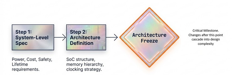
System specification to architecture freeze flow
- Phase 2: RTL development and verification
Once architecture is frozen, execution shifts to micro-architecture definition and RTL implementation. Design service providers translate architectural intent into synthesizable logic, defining data paths, control structures, interfaces, and clocking behavior.
Verification runs in parallel and expands in scope as integration progresses. Early efforts focus on block-level validation using directed tests. As blocks are integrated, subsystem-level verification exposes issues related to shared clocks, resets, and resource arbitration. System-level verification, often using emulation or FPGA platforms, validates behavior under realistic workloads.
A key responsibility in this phase is maintaining continuous feedback between design and verification. Verification readiness is measured by requirement traceability and coverage closure, not by simulation pass counts alone. Providers help prevent late surprises by ensuring issues surface when change is still manageable.
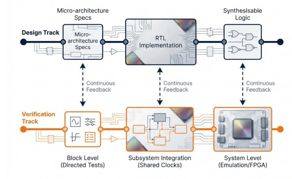
Parallel RTL design and verification track
- Phase 3: Physical design to tapeout
Physical design is where logical intent is mapped into physical geometry. Design service providers take ownership of floorplanning, defining die size, macro placement, and power grid structure to support timing, power, and thermal goals.
Placement and routing refine the design to meet performance, power, and area targets under real process constraints. Clock tree synthesis, signal integrity analysis, and power integrity checks expose interactions that are invisible at the RTL level. Sign-off confirms timing closure, IR drop, signal integrity, and manufacturability.
Netlists freeze and tapeout mark the point of no return. At this stage, finalized design data is handed off to the foundry. Errors discovered after this milestone carry a high cost and schedule impact. Design service providers reduce this risk by aligning physical execution closely with earlier architectural assumptions.
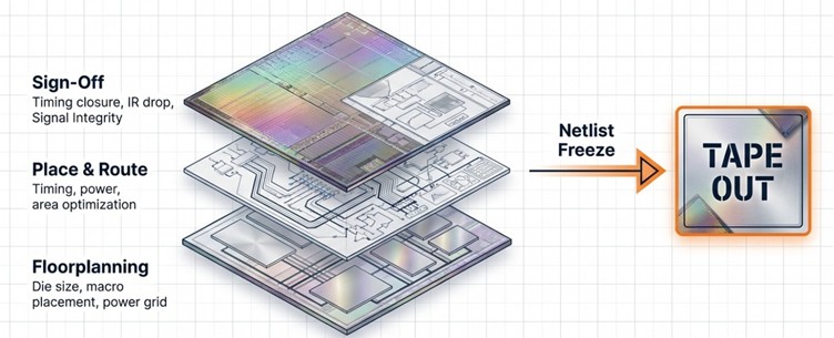
Physical design stack leading to tapeout
- Phase 4: Post-silicon to volume production
After fabrication and assembly, the program enters post-silicon validation. Design service providers support bring-up by validating clocks, resets, and basic functionality on first silicon. Characterization follows, measuring performance, power, and reliability across voltage, temperature, and frequency limits.
Post-silicon findings often trigger a reality check. Some issues are resolved through firmware workarounds or test updates, while others require metal ECOs. Yield optimization uses root-cause analysis to improve manufacturing efficiency and stability.
Once the device meets qualification criteria, it transitions into volume production. Providers continue to support yield monitoring, test refinement, and lifecycle management to ensure predictable supply and long-term reliability.
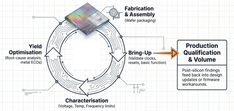
Post-Silicon feedback loop to volume production
Across all phases, the defining value of a semiconductor design service provider is traceability and ownership. Intent set during specification is carried through RTL, verification, physical implementation, and manufacturing without being diluted at handoff points.
Rather than treating each phase as an isolated activity, providers manage silicon development as a connected system. This approach reduces late-stage surprises, improves schedule predictability, and enables successful turnkey ASIC execution from concept to volume production.
Future of Silicon design
The direction of silicon design becomes clearer when viewed through changes in EDA tooling and integration models.
AI-assisted EDA increasingly shapes the architecture decisions early. Tools now guide floorplanning, timing optimization, power analysis, and verification by learning from prior designs. The impact is faster visibility, allowing teams to evaluate performance, power, and verification implications early, before architectural choices become difficult to change at a later stage.
On the other hand, chiplet-based design changes how systems scale at the architectural level. Partitioning functionality across dies allows designers to separate compute, memory, and I/O concerns while reusing proven blocks across product lines. This approach enables more flexible systems composition and faster iteration during architectural design. As a result, decisions regarding inter-die communication, latency, and power behavior significantly influence the software structure and verification strategy much earlier in the design process.
RISC-V cores increasingly appear in new CPU and GPU designs as companies look for more control over how compute behaves. The open instruction set allows designers to customize cores and add only what the workload needs. In CPUs, this helps align software and hardware more closely. In GPUs and accelerators, RISC-V often supports control and coordination alongside parallel compute blocks.
MosChip Technologies works across the silicon design and development lifecycle, supporting programs that range from RTL to volume production. Its expertise includes turnkey ASIC execution, silicon design and layout – analog and mixed-signal, physical design, and IP integration, porting, and customization. MosChip supports designs across process nodes from 180nm to 2nm and is also TSMC’s Design Center Alliance (DCA) partner.